Die4LASER.com
The (archived) guide to soldering grains of sand
To contact the author you can email me at…

27/August/07 D4Sparks – a ZVS transformer driver for Flyback Transformers and MOTs. D4Sparks page
7/March/07 Die4Thing – a laser power meter display head and micro-hotplate controller. D4Thing page.
26/December/06 Happy Holidays! – I’ve been playing with a sealed CO2 laser. A few pics and some video clips are here.
4th/April/06 – Die4Drive – a 1A laser diode driver
5/Jan/06 – Built a Laser Projector – pics are here.
21/Nov/2005 – Added the dissection of a DVD writer.
31/Oct/2005 – Added the Die4DAC area.
5/Feb/2003 – No time to update at the moment – so just dumping a few photos of interest.
http://www.die4laser.com/thedump.html
First off you are going to need some specialist equipment:
Stereo Microscope, preferably zoom type. (Very difficult without one of these)
Hot Plate, adjustable around 110C
Some method of cooling the hot plate – fan, running water, T.E. etc.
Wooden shafted Q-tips
High temperature oxygen free copper slab or bare c-mount
Indalloy 93C melting solder.
Flux - liquid Rosin type (I tried the flux that came with the Indalloy solder from SRO. On bare copper the flux did not work at all.)
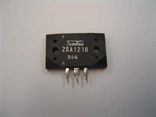
If you cannot bring yourself to spend $30 ish on 0.7 grams of gold plated copper (c-mount) or your local engineering material store has a minimum order of 1kg of HTOFC then there is another way. You can reclaim the heat spreader from large transistors. (Just check that they are cheap silicon power devices and not Beryllia filled RF power transistors.)
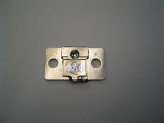
First take the donor device
Then distress it. I used a large pair of pliers as a hammer and a vice body as an anvil.
NB. Eye protection is mandatory here.
Poor thing. You can see the remains of the transistor die in the middle.
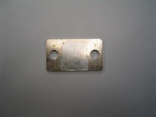
Heat the copper block up to 350C and clean off any solder.
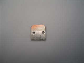
Cut to size and drill mounting holes as required.
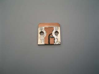
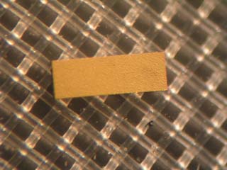
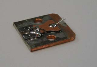
A piece of double sided PCB material is soldered onto the copper slab by heating the whole assembly with a soldering iron. The PCB material has a gap etched or cut in the top surface to form two isolated pads. A wire is soldered from the right pad to the body of the copper slab.
It is important that the edge of the mount is finished to a sharp square clean edge where the die will be mounted.
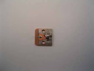
A piece of 0.25mm wire is soldered onto the edge of the PCB material. Bend this wire vertical so it is out of the way during later operations. If you intend to use the diode for CW operation only then you can add static protection consisting of a 10nF X7R 0805 capacitor, 470pf C0G 0805 capacitor and a 100R 0805 resistor. If you want pulsed operation solder a piece of wire between the two pads to short them together. This shorting link should only be cut when the diode assembly is mounted and connected to your driver circuit.
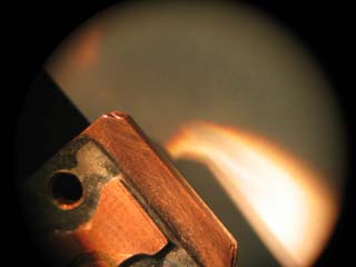
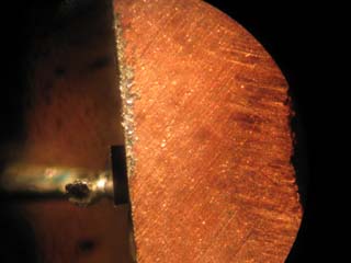
This is a 3W 808nm die. The mirror finish and parallel lines indicate that this side is the anode (+) and the lines run in the same direction as the cavity.
The laser cavity is on this side of the die and this is the side that must be well cooled.
The same die turned over. The slightly dull sputtered finish indicates that this is the cathode (-) side.
The gauze behind the die is the top surface of a gell-pack. There is a clear tacky gell that protrudes slightly through the gauze. The die is then stuck to this surface. The correct way to release the die is to connect a vacuum pump to a small hole in the rear of the plastic frame that holds the gell and gauze. This causes the gell to be sucked back through the gauze, hence releasing the die. If you do not have a vacuum pump the die may be released (at your own risk) by carefully prizing a corner of the die up from the gell with a suitable probe. *
- Suitable probes include wooden cocktail sticks, cactus needles, or my personal favorite the sharpened wooden q-tip. Anything metallic is an absolute no-no.
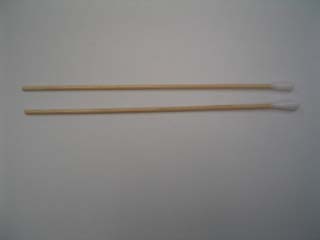
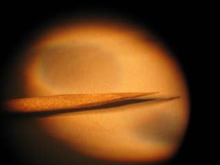
Wooden q-tips – 2 tools in one. Sharpen one end and it is perfect for manipulating die, the other is great for moving flux around over the die mount.
Talking about the die mount – it must be tinned prior to mounting the die. This requires a hotplate.
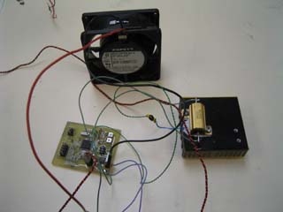
A real rough and ready set up. A pic16F877 micro, power MOSFET, 3.9Ohm 25W resistor mounted on a heatsink, precision thermistor and a fan.
The micro maintains the heatsink at 110C with the fan stopped or the micro turns off the heater and turns the fan on to cool the heatsink. The micro board was one I had from a previous project. The same functionality could be obtained from a potentiometer, thermistor, comparator and MOSFET. There are several designs on the web for small hotplates so I will refrain from publishing full details of this one. The heatsink has a couple of threaded holes added to secure the die mount to whilst soldering.
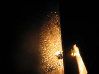
Now screw the die mount to the hotplate, heat to 110C and tin the area where the die will be mounted. Here you will need some flux, the solder and a q-tip.
Liquid rosin flux – its colour distinguishes it from practically all other fluxes.
A small piece of indalloy 93C melting solder. I prefer to roll it flat and cut it up into thinner strips lengthways. This makes it easier to use if you decide to solder the die bonding wire.
Add a little flux (0.2 of a drop – a syringe and fine nozzle makes dispensing the flux easier. Then add the solder – build up a little bead – don’t worry at this stage that it does not flow as quickly as normal solder.
Move the solder around using a flux soaked q-tip – make sure it tins right up to the edge.
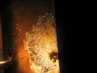
Apply a little more flux and wipe all of the solder bead off the mount. Apply a very small bead (same size as the die) at the edge of the mount.
If you are not ready immediately to drop the die on it may be worth letting the mount cool. The solder seems to oxidize a little if left for more than 5 minutes or so at 110C. You can always wipe the solder off, apply more flux and replace the bead if the surface of the solder starts to look a little dull. Now you need the die.
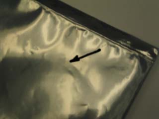
I have persuaded a die from the gel pack whilst it was over an anti-static bag *. I was tempted to make this picture part of a spot the die competition ;)
- The way to make sure you do not kill your die due to static discharge is to make sure that two surfaces are at the same potential before transferring the die (or any sensitive device from one surface to the other. This need not include hundreds of $$ of anti-static mats, humidity control and operator grounding wrist-straps although if you have them to hand it helps. If you do not have all the anti-static gear the human body can be the perfect shorting link to prevent discharge or the worst charged body to supply a discharge from. The only difference is the order in which you touch things.
- Example method for moving device from conductive surface A to conductive surface B. Touch surface A. Whilst holding surface A pick up device. Let go of surface A. Touch surface B. Whilst holding surface B place device on surface B. Let go of device. Let go of surface B.
Now the tricky bit. How go you get the die onto the mount?
Non-mar tweezers ? …. NO …. The die WILL slip and get launched over to the far side of the lab.
Vacuum pick up tool?.. Fine if you have one (and a vacuum head small enough) $$$ if you need to buy one
Or you could try flux !!!
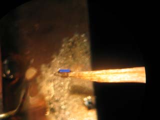
To a die flux is the second stickiest thing on the planet. A sharpened wooden q-tip dipped in a little liquid rosin flux will cause the die to stick to it. Gently touch the cathode side of the die – you can then inspect the die under a microscope to identify the cavity direction and output coupler side. The die in this picture is a very small 1.5W 808nm multimode.
That blue/ purple reflection (808nm die only) indicates that this side is the output coupler. The die supplier will be able to help you with the appearance of the o/c coating for other wavelengths.
Remember I said flux was the second stickiest thing on the planet, well the surface tension on molten solder is the only thing with more grab. Gently touch the anode side to the top of the solder bead and the die will be grabbed by the bead and will remain there when the q-tip is removed. Make sure the o/c is facing out from the edge of the mount.
The die is down. Position it such that the o/c edge of the die is coincident with the edge of the mount. A pair of sharpened q-tips make positioning the die easier. A colleague or a footswitch to enable the mount cooling cycle on your hotplate comes in handy here. Now is where the rosin flux excels – it is highly soluble in IPA (iso-propyl alcohol) or in any residue free flux cleaner (Electrolube FLU Fluxclene is my favourite – great citrus smell too.) Drop 20 drops of fluxclene onto the die. This will remove most of the flux residue. This is merely to enable inspection of the solder joint and clean the cathode side of the die.
Now form the die bonding wire
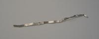
The wire is cut 2mm longer than the edge of the mount and the end is then formed into a hook so that it is a rounded edge that will touch the cathode side of the die
Carefully bend the wire down towards the die. By holding the wire away from the die at the die end with a q-tip and bending it down towards the die with a pair of tweezers at the PCB end it is possible to cause the wire to gently spring against the cathode side when released. Practice this several times on mount with no die attached. Now you have 3 choices for making the cathode connection.
1) Conductive silver ink/paint may be transferred to the die/bonding wire junction on the end of a sharpened q-tip. This works well and mistakes are recoverable. If you miss and end up shorting anode to cathode by bridging the die the ink can be removed by running the die under drips of fluxclene before the ink dries. The finished joint is however brittle and may fail if the mount is subjected to thermal cycling.
2) Conductive silver epoxy. I have not tried this. Mistakes are probably not recoverable. The epoxy will by more viscous so may be harder to transfer onto the die/wire joint – but the finished result would be more rugged.
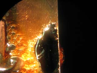
3) Solder. If you have managed to stress the bonding wire correctly and it is gently pressing down on the cathode side of the die – you can solder the bonding wire without disturbing the anode joint. Simply heat to 110C on the hotplate. Apply a little flux near to the die – the flux will boil initially and spread over the die. Touch the bonding wire with a thin sliver of solder. Surface tension will cause a bridge of solder between the bonding wire and die. If the die moves it may be repositioned before cooling using the q-tips as mentioned earlier.
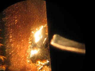
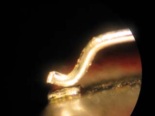
End view showing the o/c and bonding wire to cathode solder joint. (the die is a 1.5W 808nm, the wire is 0.25mm diameter)
Now it just remains to clean up boil in IPA / acetone for a couple of minutes – although I have found dripping 100 drops of fluxclene onto the o/c is adequate (rosin flux is highly soluble and visual signs of it disappear after the first 5 drops. It is worthwhile checking the o/c under the microscope to check for any signs of contamination.
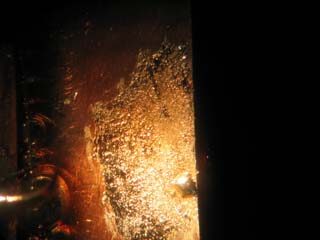
It only remains now to test the beast.
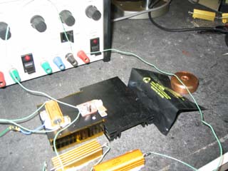
The hotplate with no power connected makes a reasonable heatsink for brief operation. The PSU is a standard adjustable lab one. It has been checked to see that it behaves itself – no surprises due to dirty potentiometers. The PSU is used in Voltage mode. There are two 1ohm resistors in series with the die. Initially the die is shorted out. The PSU is enabled and the o/p voltage set to 0v. The shorting link is removed and the voltage is slowly turned up. The current was monitored and the voltage set to give a current of 1A. This corresponds to an output power of just under 1watt. (I didn’t want to run the diode too hard because there was no airflow across the vanes of the heatsink.
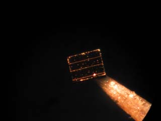
Now – one of those Casix hybrid DPSS crystals later (plus a homebuilt smps laser diode driver and an old telescope as a collimator) and hey-presto – the laser pointer from hell ;)
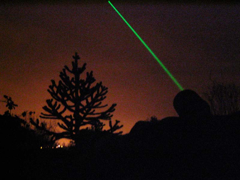
The beam terminates on low cloud.
Thanks and appreciation to:
Bob from the alt-lasers newsgroup – for moral support, pearls of wisdom and most of all the laser die.
Sam for the excellent LASERFAQ
Usual disclaimer – If you blind yourself it’s not my fault – use appropriate protective eyewear – if in doubt don’t do it.
Best Regards,
Robin